

What Is Thick Film Hybrid Manufacturing?
Thick Film Hybrid manufacturing builds conductive and resistive features on ceramic substrates for compact, stable, and demanding electronic applications.
27 August 2026 · 5 minute read
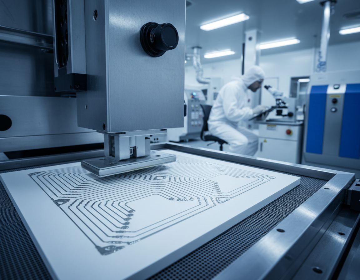
Electronic functions printed onto ceramic
In thick film manufacturing, formulated conductive, resistive, and insulating materials are deposited onto a ceramic substrate. Each layer is printed in a controlled pattern and fired at high temperature to create a durable circuit structure.
Discrete components or semiconductor devices can then be attached and interconnected to form a compact hybrid assembly.
From artwork to a tuned circuit
The typical pathway includes substrate preparation, screen printing, drying, firing, inspection, component attachment, interconnection, and protective finishing. Where the design uses printed resistors, laser trimming can adjust resistance to the required target.
The exact material system and process sequence depend on electrical, thermal, mechanical, and environmental requirements.
Where the technology earns its place
Ceramic substrates can provide useful thermal performance, dimensional stability, and compatibility with compact circuit construction. Thick film hybrids are therefore considered for specialist sensing, control, power, instrumentation, and rugged applications.
Technology selection should be based on the full requirement. Conventional PCBs remain the right answer for many products; a hybrid becomes valuable when its material and construction advantages solve a real design constraint.
Bring us the requirement, the design, or the production challenge.
Tell us what you are building, where the project currently sits, the expected quantities and the timing. We typically respond within 24 hours.